The wafer measurement instrument offering the best available calibrated analysis of carrier recombination lifetime. Fully compliant with SEMI Standard PV-13.
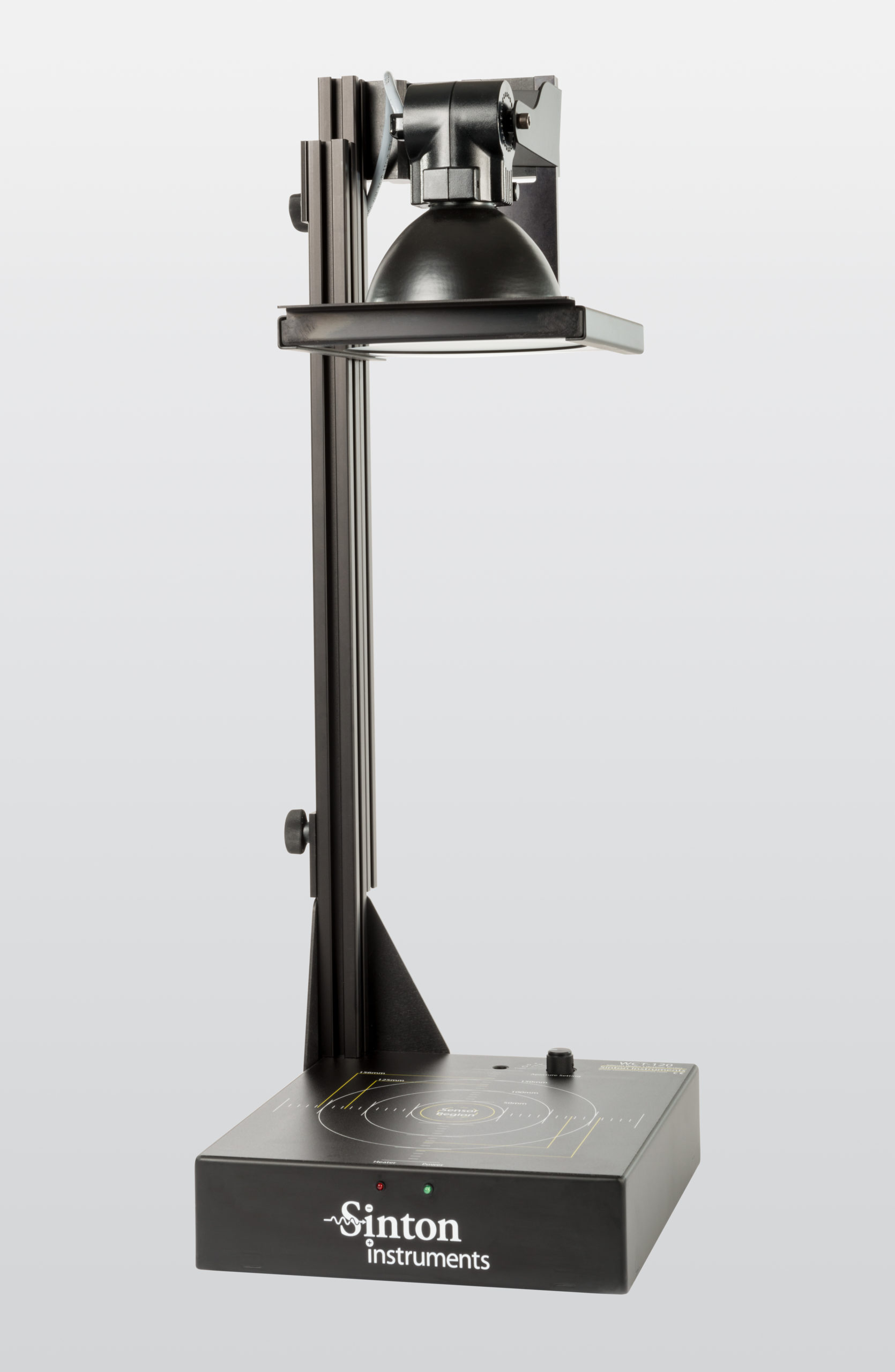
The WCT-120 is an affordable, tabletop silicon lifetime and wafer metrology system, suitable for both device research and industrial process control. The WCT-120MX is optimized for 230mm wafer measurements.
Product Overview
WCT-120 and WCT-120MX instruments showcase our unique measurement and analysis techniques, including the highly regarded Quasi-Steady-State Photoconductance (QSSPC) lifetime measurement method developed by Sinton Instruments in 1994.
The WCT-120 instruments utilize both the QSSPC and transient photoconductance decay techniques to measure the lifetimes of wafers in the range of 10ns to greater than 10ms. The QSSPC technique is ideal for monitoring multicrystalline wafers, dopant diffusions, and low lifetime samples. The transient photoconductance decay technique is ideal for monitoring high lifetime samples at various processing steps.
The WCT-120 lifetime measurement also yields the implied open-circuit voltage (versus illumination) curve, which is comparable to an I-V curve at each stage of a solar cell process.
WCT System Capabilities
Primary application:
Step-by-step monitoring and optimization of a fabrication process.
Other Applications:
- Monitoring initial material quality
- Detecting heavy metals contamination during wafer processing
- Evaluating surface passivation and emitter dopant diffusion
- Evaluating process-induced shunting using the implied I-V measurement
Further Information
For key features, specifications, and additional information, download the WCT-120 product note (PDF – 563k).
Request A Quote
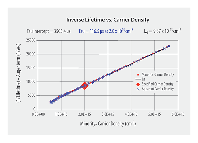
Sinton Instruments’ analysis yields a calibrated carrier injection level for each wafer, so you can interpret lifetime data in a physically precise way. Specific parameters of interest are displayed and logged for each measurement.
